

High Quality Wafer Cleaning System Enhances Semiconductor Manufacturing Reliability
2026-10-16
In semiconductor manufacturing, even microscopic contamination can compromise yield and long-term device reliability. High-quality wafer cleaning is no longer optional—it’s a critical control point. Siansonic brings precision-engineered cleaning technology that removes particles and residues without damaging delicate structures, helping fabs sustain consistent output. This post explores how advanced wafer cleaning systems directly strengthen manufacturing dependability and why subtle engineering differences matter more than ever.
Why a Single Nanoparticle Can Decide Wafer Reliability
In advanced semiconductor manufacturing, the margin for error has shrunk to dimensions smaller than a virus. A single nanoparticle—often no larger than a few nanometers—can land in a critical spot during lithography, etching, or deposition. Once there, it disrupts the intended pattern, creating a bridge between adjacent lines or a void in a gate dielectric. Modern fabs spend enormous effort filtering cleanroom air and monitoring particle counts precisely because one stray particle can turn a potentially functional die into scrap.
The location of the particle matters more than its size. A particle resting on an open field region may be harmless, but the same particle positioned over a transistor channel or a via opening can cause immediate failure. As device geometries approach 3nm and below, even sub-10nm particles become comparable to feature sizes. This means the traditional approach of relying on statistical defect density no longer captures the risk: a single event can dominate yield loss on an entire wafer if it hits a repeated pattern area.
Reliability testing often reveals these latent defects only after stress conditions—temperature cycling, voltage bias, or moisture exposure. A particle trapped inside a low-k dielectric can accelerate electromigration or time-dependent dielectric breakdown. Thus, wafer reliability is not just a function of average cleanliness; it hinges on eliminating those rare, high-impact particles. Engineers now use inline inspection tools with sub-nanometer sensitivity, because missing one particle can mean the difference between a reliable product and a field failure.
Fluid Mechanics as a Yield Booster in Wafer Cleaning
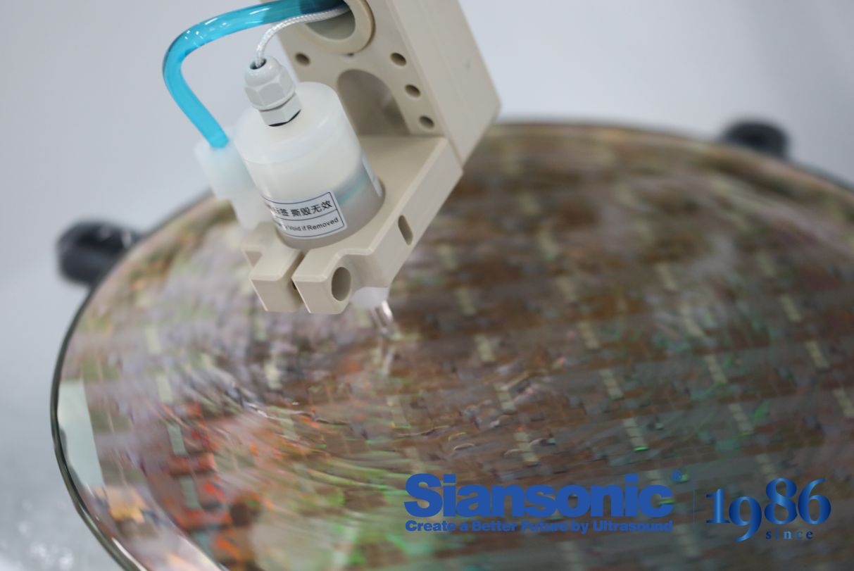
Fluid mechanics plays a surprisingly direct role in the economics of wafer cleaning. Even marginal improvements in how cleaning fluids move across a wafer surface can lift overall yield by reducing defect densities and rework rates. Rather than treating cleaning as a purely chemical step, fabs that tune flow regimes—laminar versus transitional, impingement angle, and rinse uniformity—often see measurable gains in particle removal efficiency without adding process time.
The yield-boosting mechanism is twofold. First, controlled shear stress at the wafer interface dislodges submicron contaminants that static or low-flow chemistries leave behind. Second, optimized fluid delivery prevents redeposition by carrying particles away from the surface before they can reattach. This is especially relevant for high-aspect-ratio structures, where inadequate fluid exchange is a common hidden yield killer. Simple adjustments like nozzle geometry, flow pulsing, or targeted acoustic streaming can shift the cleaning step from a bottleneck to a subtle yield lever.
Practically, engineers who treat fluid mechanics as a design parameter rather than a fixed utility report fewer micro-scratches, lower defect counts post-clean, and more stable electrical test results. The return is not just higher bin yields but also reduced variability wafer-to-wafer and lot-to-lot. In advanced nodes, where every particle counts, mastering the flow is often the difference between hitting yield targets and chasing excursions.
Cleaning Chemistries That Keep Pace With Advanced Node Materials
At the 2nm node and below, cleaning steps are no longer a generic front-end-of-line afterthought. Gate-all-around nanosheet stacks, buried power rails, and backside power delivery introduce metals like molybdenum and ruthenium next to ultra-thin low-k dielectrics, so a wet clean that removes polymer residue without attacking the conductor is a moving target. Suppliers now balance chelator strength, pH, and water activity so the chemistry forms a transient passivation film on exposed metal surfaces while loosening fluorinated etch byproducts. This passivation is what prevents galvanic corrosion between dissimilar metals during the rinse, a failure mode that rarely mattered at older nodes but now shows up as nanosheet line breaks or contact opens.
EUV patterning has pushed cleaning chemistry further away from conventional sulfuric-peroxide and SC1/SC2 recipes. Metal-oxide resists and spin-on underlayers leave behind cross-linked, metal-containing residues that are not easily lifted by standard oxidizers. Fabs are adopting fluoride-free stripper blends with tailored surfactants and chelators that keep particles suspended and prevent re-deposition on high-aspect-ratio fin and nanosheet surfaces. In addition, low-water, solvent-rich formulations help penetrate narrow trenches without swelling or damaging ultra-low-k spacers. On the tool side, wet benches with in-line concentration and particle monitoring can feed data back to chemical dosing, letting the clean step adapt to incoming film variations instead of relying on a fixed time-and-temperature recipe.
Rethinking Contaminant Removal Paths From Bath to Spray
In many cleaning and surface preparation processes, the default assumption has long been that immersing parts in a chemical bath provides the most thorough contaminant removal. Yet this approach frequently suffers from stagnant boundary layers, redeposition of particles, and a steady decline in bath purity as residues accumulate. Rethinking the path from bath to spray forces a closer look at how contaminants actually detach from surfaces—and whether a continuous, directed flow can outperform a static soak.
Spray-based removal introduces a fundamentally different transport mechanism. Rather than relying on diffusion and gentle agitation within a liquid volume, droplets impact the surface with measurable kinetic energy, disrupting adherent films and dislodging particles through shear and impingement. This shift also changes the chemistry economics: a spray system can operate with lower total chemical inventory and generate less hazardous waste, since fresh solution is delivered on demand instead of being reused until exhausted.
Of course, moving from bath to spray is not simply a matter of swapping hardware. Nozzle geometry, spray angle, droplet size distribution, and impact velocity all influence whether the process achieves uniform coverage or leaves shadowed regions untouched. Understanding these variables allows engineers to design contaminant removal paths that are more predictable, more resource-efficient, and better suited to complex part geometries than traditional immersion ever could.
Measuring What Matters Beyond Particle Counts in Fab Data
Particle counts alone paint an incomplete picture on a modern fab floor. Two wafers can report the same total defect tally yet present radically different yield risks. A cluster of sub-50nm particles near a critical gate region is far more dangerous than a dozen larger particles on a non-functional scribe line. Process engineers therefore need to shift attention toward spatial distribution, particle size histograms, and compositional signatures. Only by separating killer defects from cosmetic anomalies can teams allocate inspection and review resources effectively.
Time-resolved data adds another layer that static counts miss. A sudden spike in particles during a specific chamber conditioning step points to a gas delivery or exhaust imbalance, while a gradual upward drift may indicate quartz wear or a degraded filter. Tracking particle events against tool maintenance logs, recipe changes, and wafer lot history reveals patterns that raw totals obscure. This chronological view turns defect data into a diagnostic trail rather than a post-mortem count.
Beyond physical attributes, fab data should capture the economics of defectivity. Kill ratio, or the probability that a particle of a given size and location causes electrical failure, links inspection results directly to yield impact. Models that integrate defect coordinates with design layout and process margins produce a risk score far more actionable than a simple particle count. Measuring what matters means prioritizing the defects that actually threaten product quality, not just the ones that are easiest to count.
Turning Repeatable Cleanliness Into a Production Reality
Repeatable cleanliness in production doesn't come from occasional deep cleans or relying on operator vigilance alone. It requires a locked sequence of chemical concentration, temperature, contact time, and mechanical action that can be executed the same way every shift. When any one of these parameters drifts, residues stay behind even if surfaces appear clean to the naked eye.
The real shift happens when verification moves from visual inspection to measurable output. Swab tests, rinse water analysis, and ATP monitoring convert cleanliness into a pass-or-fail number that leaves no room for interpretation. Equipment design also plays a quiet but decisive role: dead legs, rough welds, and shadow zones can shelter contamination and defeat an otherwise sound procedure.
Making this stick means treating deviations as signals rather than one-off events. Trends in residue levels or bioburden counts should prompt a root-cause review and adjustment of the cleaning cycle, not just a retest. Over time, the process stops being a reaction to failures and becomes a prevention routine, so repeatable cleanliness turns into a standard production output instead of an aspiration.
FAQ
It comes down to how precisely the system controls particle removal without introducing new defects. A well-engineered platform maintains uniform chemical dispensing, controls megasonic energy distribution, and avoids cross-contamination between chambers. You also want real-time monitoring of bath life and rinse resistivity, because subtle variations there can quietly erode yield.
Reliability in semiconductor manufacturing isn't just about final test pass rates; it's about repeatability across every lot. Any residue left on a wafer can become a latent defect that shows up later as a field failure. A high-quality cleaning step removes the root cause of those intermittent issues before they ever reach packaging.
They've shifted away from brute-force scrubbing toward highly tuned chemical and mechanical action. For example, aerosol jet cleaning and dilute chemistries can lift nanoscale particles without collapsing high-aspect-ratio features. The real craftsmanship is in matching the energy input to the surface sensitivity, which older batch tools simply couldn't do.
Yes, but the savings show up in less obvious places. Fewer rework loops, shorter queue times at inspection, and a drop in scrapped wafers all reduce cost per good die. You might pay more upfront for the tool, but the sustained improvement in line yield typically outweighs that within a few quarters.
It's rarely the large particles people can see under a microscope. Sub-20nm metallic impurities and organic monolayers are now the bigger threat because they alter surface wetting and adhesion. A high-end cleaning system has to target those invisible contaminants while also keeping particle counts extremely low.
Single-wafer processing with cryogenic aerosol cleaning and advanced dilute chemistries are picking up momentum. They allow rapid switching between recipes and tighter control over etch rates on sensitive films. Batch immersion still has its place for certain applications, but the trend leans toward platforms that can adjust energy and chemistry per wafer.
They run split-lot tests with deliberately contaminated wafers and measure defect density before and after cleaning. Some also use short-loop test vehicles with embedded structures that mimic real product. The key is looking at electrical yield impact, not just particle removal efficiency, because a clean surface that has been chemically damaged is still a reliability risk.
Conclusion
In advanced semiconductor fabs, a single nanoscale particle settling on a critical pattern can render an entire die useless, so the quality of wafer cleaning directly shapes manufacturing reliability. High-end cleaning tools now treat fluid mechanics as a yield lever, using controlled flow dynamics and optimized bath-to-spray transitions to lift contaminants from high-aspect-ratio structures without damaging fragile films. At the same time, cleaning chemistries must evolve alongside new materials such as cobalt, ruthenium, and low-k dielectrics, because formulations that worked at older nodes can cause galvanic corrosion or surface roughening at 3nm and below.
Beyond simply reducing particle counts, fabs are integrating more meaningful wafer-level data—defect maps, surface morphology, and electrical test correlations—to judge cleaning effectiveness. This broader view helps engineers spot residue patterns that conventional particle monitors miss. When such measurements feed back into tool recipes, repeatable cleanliness becomes a production reality rather than a hope. The result is a wafer cleaning system that not only removes contaminants but stabilizes yield, extends equipment uptime, and strengthens the overall reliability of semiconductor manufacturing.
Contact Us
Contact Person: Ivy Zhang
Email: [email protected]
Tel/WhatsApp: +86 1081502288
Website: https://www.siansonic.com/