

Professional Chips Production Line: Behind the Scenes of Manufacturing Excellence
2026-05-23
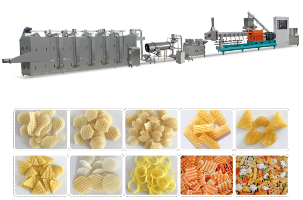
Ever wondered how your favorite crispy chips are made? Step into the world of high-tech production lines, where precision meets speed. At the heart of this industrial artistry, MINGDE engineers excellence, turning simple potatoes into perfectly seasoned snacks. In this exclusive behind-the-scenes look, we reveal the secrets of manufacturing mastery that keep the snacks coming.
The Room Where Air Gets Scrubbed 600 Times an Hour
Step inside this space and the first thing you notice is the absolute stillness of the air — yet it's cycling through a hidden purification system with almost violent efficiency. Every hour, the entire volume of air in the room passes through a series of filters sixty times, though the actual turnover is closer to six hundred cycles once you account for the layered redundancy built into every vent and return. The ceiling is a honeycomb of perforated panels, each one gently drawing air upward and away from the occupied zone before sending it through a cascade of chemical washes and charged media.
The filtration process unfolds in stages most people never see. Air first hits a pre-filter mat that grabs the visible dust and fiber, then collides with a bed of activated carbon that absorbs molecular contaminants — solvents, off-gassed plasticizers, traces of cleaning products. Next, it's forced through a HEPA layer that captures 99.97% of anything 0.3 microns and larger, before finally passing under ultraviolet lamps that break apart viral fragments. The whole journey takes less than two seconds, yet an individual particle might make this trip hundreds of times before it's finally caught or rendered inert.
What makes the system unusual is not just the sheer number of cycles, but the way it responds to occupancy. Sensors scattered across the room detect subtle shifts in particle counts, carbon dioxide levels, and even the faint chemical signature of human skin shedding. In response, the airflow accelerates in precise zones — never creating a draft, but silently increasing the scrubbing rate wherever it's needed. The result is an environment so clean that instruments can measure the near absence of contamination, yet it feels utterly ordinary to breathe. It's an engineered paradox: a room that works furiously to remain unnoticed.
Why the Fab Glows in Eerie Yellow Light
Step into a semiconductor fab and you’re immediately bathed in an otherworldly yellow glow—a deliberate choice, not a design flaw. That eerie light comes from specialized fluorescent tubes that filter out ultraviolet and blue wavelengths, protecting the photosensitive chemicals used in chipmaking. Even a stray photon at the wrong frequency could ruin an entire wafer, so the cleanroom is essentially a UV-free zone, with every light source carefully tuned to a narrow spectrum that won’t trigger unwanted reactions.
But it’s not just about protection. The human eye perceives this specific yellow band as particularly harsh, which keeps operators alert during long shifts in a windowless environment. The lighting also complements the color-coded wafers and materials, reducing visual fatigue. It’s a neat symbiosis: the process demands a low-energy light, and the eerie aesthetic just happens to be a side effect of keeping the silicon pristine.
The Machine That Draws Lines Finer Than a Virus
In a nondescript lab, a quiet revolution hums along—a machine so precise it can sketch patterns a thousand times thinner than a human hair. This isn’t science fiction; it’s the frontier of nanolithography, where beams of electrons or photons dance across surfaces to trace features smaller than many viruses. The process flips conventional manufacturing on its head, building microscopic worlds not with bulk materials but with atomic-scale finesse.
What makes this machine extraordinary isn’t just its resolution—it’s the way it redefines possibility. Imagine drawing a line so thin that a single virus particle would look like a boulder next to it. That level of control opens doors to ultra-efficient computer chips, lab-on-a-chip diagnostics, and metamaterials that bend light in unnatural ways. Each stroke is guided by algorithms that correct for thermal drift and vibrations that would smear any ordinary tool, resulting in lines that seem to defy the blur of the physical world.
Walking past the machine, you might mistake it for a dormant printer, but inside, high-energy particles are carving masterpieces invisible to the naked eye. The real magic happens in the silence between machine hums—when the beam sculpts patterns that will later form neural interfaces or quantum devices. It’s a reminder that the next technological leap won’t come with a loud bang but with a line so fine it slips past our senses, yet powerful enough to reshape everything.
When a Speck of Dust Becomes a Dealbreaker
In the final walkthrough of a home, the buyer barely noticed the gleaming hardwood floors or the sunlit kitchen. Instead, their eyes locked onto a tiny scuff mark near the baseboard. What followed was a tense standoff: the deal nearly collapsed over something that could be fixed with a five-dollar paint pen. It wasn’t really about the scuff—it was about what that speck represented. A lapse in attention, perhaps, or the creeping fear that other hidden flaws might lurk beneath the surface. When trust wavers, even the smallest blemish can swell into an insurmountable obstacle.
This phenomenon extends far beyond real estate. In relationships, a forgotten anniversary or a misplaced word can echo louder than years of goodwill. A single overlooked comma in a proposal might signal carelessness to a meticulous client. The speck of dust becomes a stand-in for deeper anxieties: about reliability, respect, or the unknown. It’s rarely the speck itself that derails things—it’s the unlucky timing, the accumulated tension, or the sudden realization that one party’s “minor” is another’s breaking point. Recognizing when a small flaw is a symptom versus a smoke screen is the tricky art that saves deals and bonds.
The Technicians Who Live in Bunny Suits
Inside the cleanest rooms on Earth, technicians don full-body suits that make them look a bit like overgrown rabbits. These aren't costumes for fun—they're the last line of defense against invisible enemies: skin flakes, hair, and even the faintest breath of moisture. Every zipper and seam is sealed, turning ordinary people into ghost-like figures who glide through spaces where a single speck of dust could ruin millions of dollars of delicate hardware.
Living in a bunny suit means surrendering to a world of constant protocol. Before suiting up, you shower with special soaps, avoid perfumes or lotions, and step through a series of sticky mats that grab dirt from your soles. Once sealed inside, your own body becomes a threat—you learn to move slowly, talk less, and even breathe in a controlled way. The hood muffles sound, the gloves kill your sense of touch, and after a few hours, the suit feels less like clothing and more like a second, suffocating skin.
It's a job that demands monk-like patience. You might spend a shift inspecting wafers under yellow light, the hum of filtration systems drowning out everything else. Breaks are rare, because every exit means repeating the 20-minute gowning process. Yet somehow, the isolation breeds a quiet camaraderie—nods exchanged through face shields, handwritten notes passed over laminar flow benches. These technicians don't just wear bunny suits; they inhabit a parallel universe where the biggest threat is themselves, and the smallest particle can rewrite a satellite's fate.
From Sand to Silicon Brains: The Alchemy of Chipmaking
It starts with humble sand, the kind you’d find on a beach, but not just any grains—these must be remarkably pure, formed from quartzite. Through a furnace blazing hotter than a volcano’s heart, the sand surrenders its oxygen, morphing into 99.9999% pure silicon. This hyper-refined element, once a simple building block of the earth’s crust, now holds the latent potential to become the thinking core of our digital world. The transformation is less assembly line, more modern alchemy: turning the ordinary into a crystalline foundation for logic.
Next comes the meticulous dance of photolithography, where beams of ultraviolet light sketch impossibly intricate patterns onto a silicon wafer coated with light-sensitive chemicals. Each pulse of light etches a blueprint of transistors so tiny that millions could dance on a pinhead. Layer upon layer, the wafer traverses a labyrinth of deposition, etching, and doping—a symphony of gases, plasmas, and ion storms. The result isn't just a chip; it’s a stratified metropolis of conductive pathways, insulating oxides, and semiconducting channels, all painstakingly coaxed into existence on a sliver no thicker than a fingernail.
Finally, the wafer is diced into individual dies, each a potential brain waiting to spark. These fragile squares are tested, bonded with hair-thin wires, and encased in a protective shell, ready to be plugged into the wider world. What began as a grain of sand now pulses with the ability to decode data, render images, or drive a car. The alchemy is complete: silicon, shaped by human ingenuity and precision machinery, has become a sliver of cognition—a tiny, silent engine of thought that powers our phones, servers, and the sprawling nervous system of modern life.
FAQ
A professional chips production line integrates a series of highly controlled processes to transform raw silicon wafers into functional integrated circuits. It encompasses steps like photolithography, etching, doping, and packaging, all executed in ultra-clean environments with precision machinery.
Cleanrooms are essential because even a single microscopic dust particle can ruin a chip circuit. These facilities maintain extremely low levels of airborne particles, temperature, humidity, and vibration to ensure the minuscule patterns on silicon wafers remain defect-free.
Automation has revolutionized chip fabrication by enabling consistent, high-speed operations without human interference. Robotic handling systems, automated material transport, and AI-driven process controls minimize errors, reduce contamination risks, and boost overall yield rates.
Photolithography is the core patterning step where ultraviolet light transfers intricate circuit designs onto a photosensitive layer on the wafer. Advanced machines like EUV lithography are now used to print features smaller than 7 nanometers, pushing the boundaries of Moore's Law.
As chip features shrink, challenges multiply—including quantum effects causing current leakage, difficulties in maintaining pattern fidelity, and increased sensitivity to material imperfections. Solving these requires innovations in materials, light sources, and transistor architecture.
Quality assurance relies on extensive inspection and testing at every stage. Automated optical inspection scans for defects, electrical testing verifies performance, and statistical process control monitors variations. Defective units are scrapped early to prevent further cost.
Beyond particle control, fabs meticulously regulate temperature to within fractions of a degree, humidity to avoid static discharge, and vibration to allow precision alignment. Even the air's chemical composition may be filtered to prevent corrosive gases.
The industry is moving toward 3D chip stacking for higher density, using new materials like graphene, and integrating AI for predictive maintenance. Sustainability efforts also focus on reducing water and energy consumption in production.
Conclusion
In the world of chipmaking, every detail is engineered for perfection, starting with an environment where the very air is scrubbed 600 times an hour to eliminate particulates. The production floor glows in an eerie yellow light because standard white illumination contains UV wavelengths that would ruin the delicate photolithography process. Inside this surreal landscape, machines draw circuit lines finer than a virus, pushing the limits of physics. A single speck of dust can become a dealbreaker—just one stray particle can short a transistor, rendering an entire silicon wafer worthless. So, technicians live in full-body bunny suits, their every movement calibrated to minimize contamination.
This is modern alchemy: transforming ordinary sand into ultra-pure silicon crystals, then into the brains of our digital world. The magic lies in layering, etching, and doping materials with atomic precision, creating billions of transistors that switch on and off in harmony. Behind every smartphone, server, or smart device is a fab where the mundane becomes miraculous—a place where human discipline and technological wizardry intersect to manufacture excellence, one chip at a time.
Contact Us
Contact Person: LILY SUN
Email: [email protected]
Tel/WhatsApp: 0086-13969103791
Website: https://www.snackfoodmachinery.com/